Welcome to ZK Electronic
16 years of industry experience
Good material qualty, high efficiency, fast delivery
搜索
NEWS
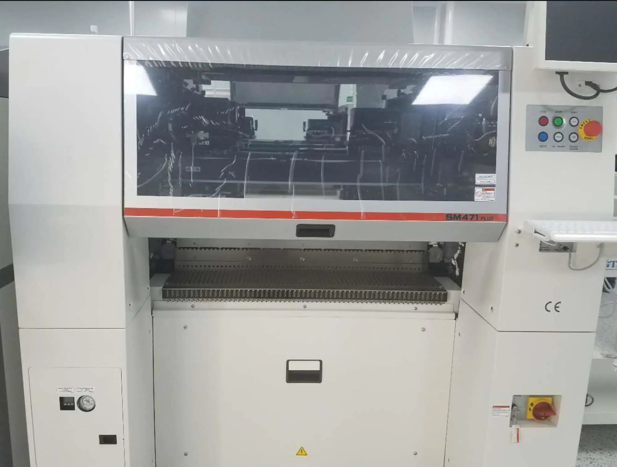
SMT Printed Solder Paste Process
- Categories:Industry News
- Author:Becky Su
- Origin:
- Time of issue:2023-07-14 11:01
- Views:
(Summary description)SMT Printed Solder Paste Process 1. Screen printing technology Screen printing technology is the use of already made stencil, with a certain method to make the screen and printing machine direct contact, and make the solder paste in the stencil uniform flow, by the mask pattern into the mesh. When the screen off the printing plate, the solder paste in the shape of the mask pattern from the mesh off to the corresponding pad graphics on the printing plate, thus completing the printing of solder paste on the printing plate. 2. Printing solder paste process inspection Printing process is to ensure the quality of the surface assembly of one of the key processes. According to statistics in the PCB design is correct, components and board quality is guaranteed under the premise of surface assembly quality problems in 70% of the quality problems in the printing process. In order to ensure the quality of SMT assembly, must strictly control the quality of printed solder paste. Printed solder paste volume requirements are as follows: ① applied amount of solder paste uniformity, consistency. Solder paste graphics to be clear, try not to stick between adjacent graphics. Solder paste graphics and pad graphics play consistent, try not to misalignment. ② In general, the amount of solder paste per unit area on the pad should be 0.8mg / 2mm or so. For narrow-pitch components, should be 0.5mg / 2mm or so (in practice, with the template thickness and opening size to control). ③ printed on the substrate of the solder paste and hope that the weight value compared to the allowable deviation, solder paste to cover the area of each pad, should be more than 75%. ④ solder paste after printing, there should be no serious collapse, edge neatly, dislocation is not greater than 0.2mm, for narrow-pitch components pads, dislocation is not greater than 0.lmm. the substrate is not allowed to be contaminated by solder paste. Visual inspection, with a narrow pitch with 2 to 5 times magnification or 3 to 20 times microscope inspection. 3. Solder paste printing defects, causes and countermeasures Excellent printing graphics should be the vertical and horizontal direction of uniformity and bracing, full, around the clean, full of solder paste pads. With such a printed graphic placement device, after reflow soldering, will get excellent welding results. (1) Misalignment of solder paste pattern Causes: improper alignment of the steel plate and pad offset; printing machine accuracy is not enough. Hazard: easy to cause bridge connection. Countermeasures: adjust the position of the steel plate; adjust the printing machine. (2) Solder paste graphics pull the tip, there are concave Causes: excessive squeegee pressure; rubber squeegee hardness is not enough; window oversized. Hazard: the amount of solder is not enough, easy to appear virtual welding, solder joint strength is not enough. Countermeasures: adjust the printing pressure; change the metal scraper; improve the template window design. (3) The amount of solder paste is too much Causes: template window size is too large; the gap between the steel plate and PCB is too large. Hazard: easy to cause bridging. Countermeasures: check the size of the template window; adjust the printing parameters, especially the gap between the PCB template. (4) uneven graphics, broken points Causes: template window wall smoothness is not good; printing plate times more than one, failed to wipe off the residual solder paste in a timely manner; paste thixotropy is not good. Hazard: easy to cause the amount of solder is insufficient, such as virtual welding defects. Countermeasures: wipe the template. (5) graphic staining Causes: stencil printing times, failed to wipe clean in time; poor quality of solder paste; steel plate left shaking. Hazard: easy to bridge. Countermeasures: scrub the steel plate; change the paste; adjust the machine. In short, solder paste printing should be aware of the parameters of the paste will change at any time, such as particle size / shape, thixotropy and flux properties. In addition, the parameters of the printing machine can also cause changes, such as printing pressure/speed and ambient temperature. The quality of solder paste printing has a great impact on solder quality, so each parameter in the printing process should be treated carefully and the relevant coefficients should be observed and recorded frequently.
SMT Printed Solder Paste Process
(Summary description)SMT Printed Solder Paste Process
1. Screen printing technology
Screen printing technology is the use of already made stencil, with a certain method to make the screen and printing machine direct contact, and make the solder paste in the stencil uniform flow, by the mask pattern into the mesh. When the screen off the printing plate, the solder paste in the shape of the mask pattern from the mesh off to the corresponding pad graphics on the printing plate, thus completing the printing of solder paste on the printing plate.
2. Printing solder paste process inspection
Printing process is to ensure the quality of the surface assembly of one of the key processes. According to statistics in the PCB design is correct, components and board quality is guaranteed under the premise of surface assembly quality problems in 70% of the quality problems in the printing process. In order to ensure the quality of SMT assembly, must strictly control the quality of printed solder paste.
Printed solder paste volume requirements are as follows:
① applied amount of solder paste uniformity, consistency. Solder paste graphics to be clear, try not to stick between adjacent graphics. Solder paste graphics and pad graphics play consistent, try not to misalignment.
② In general, the amount of solder paste per unit area on the pad should be 0.8mg / 2mm or so. For narrow-pitch components, should be 0.5mg / 2mm or so (in practice, with the template thickness and opening size to control).
③ printed on the substrate of the solder paste and hope that the weight value compared to the allowable deviation, solder paste to cover the area of each pad, should be more than 75%.
④ solder paste after printing, there should be no serious collapse, edge neatly, dislocation is not greater than 0.2mm, for narrow-pitch components pads, dislocation is not greater than 0.lmm. the substrate is not allowed to be contaminated by solder paste.
Visual inspection, with a narrow pitch with 2 to 5 times magnification or 3 to 20 times microscope inspection.
3. Solder paste printing defects, causes and countermeasures
Excellent printing graphics should be the vertical and horizontal direction of uniformity and bracing, full, around the clean, full of solder paste pads. With such a printed graphic placement device, after reflow soldering, will get excellent welding results.
(1) Misalignment of solder paste pattern
Causes: improper alignment of the steel plate and pad offset; printing machine accuracy is not enough.
Hazard: easy to cause bridge connection.
Countermeasures: adjust the position of the steel plate; adjust the printing machine.
(2) Solder paste graphics pull the tip, there are concave
Causes: excessive squeegee pressure; rubber squeegee hardness is not enough; window oversized.
Hazard: the amount of solder is not enough, easy to appear virtual welding, solder joint strength is not enough.
Countermeasures: adjust the printing pressure; change the metal scraper; improve the template window design.
(3) The amount of solder paste is too much
Causes: template window size is too large; the gap between the steel plate and PCB is too large.
Hazard: easy to cause bridging.
Countermeasures: check the size of the template window; adjust the printing parameters, especially the gap between the PCB template.
(4) uneven graphics, broken points
Causes: template window wall smoothness is not good; printing plate times more than one, failed to wipe off the residual solder paste in a timely manner; paste thixotropy is not good.
Hazard: easy to cause the amount of solder is insufficient, such as virtual welding defects.
Countermeasures: wipe the template.
(5) graphic staining
Causes: stencil printing times, failed to wipe clean in time; poor quality of solder paste; steel plate left shaking.
Hazard: easy to bridge.
Countermeasures: scrub the steel plate; change the paste; adjust the machine.
In short, solder paste printing should be aware of the parameters of the paste will change at any time, such as particle size / shape, thixotropy and flux properties. In addition, the parameters of the printing machine can also cause changes, such as printing pressure/speed and ambient temperature. The quality of solder paste printing has a great impact on solder quality, so each parameter in the printing process should be treated carefully and the relevant coefficients should be observed and recorded frequently.
- Categories:Industry News
- Author:Becky Su
- Origin:
- Time of issue:2023-07-14 11:01
- Views:
Information
SMT Printed Solder Paste Process
1. Screen printing technology
Screen printing technology is the use of already made stencil, with a certain method to make the screen and printing machine direct contact, and make the solder paste in the stencil uniform flow, by the mask pattern into the mesh. When the screen off the printing plate, the solder paste in the shape of the mask pattern from the mesh off to the corresponding pad graphics on the printing plate, thus completing the printing of solder paste on the printing plate.
2. Printing solder paste process inspection
Printing process is to ensure the quality of the surface assembly of one of the key processes. According to statistics in the PCB design is correct, components and board quality is guaranteed under the premise of surface assembly quality problems in 70% of the quality problems in the printing process. In order to ensure the quality of SMT assembly, must strictly control the quality of printed solder paste.
Printed solder paste volume requirements are as follows:
① applied amount of solder paste uniformity, consistency. Solder paste graphics to be clear, try not to stick between adjacent graphics. Solder paste graphics and pad graphics play consistent, try not to misalignment.
② In general, the amount of solder paste per unit area on the pad should be 0.8mg / 2mm or so. For narrow-pitch components, should be 0.5mg / 2mm or so (in practice, with the template thickness and opening size to control).
③ printed on the substrate of the solder paste and hope that the weight value compared to the allowable deviation, solder paste to cover the area of each pad, should be more than 75%.
④ solder paste after printing, there should be no serious collapse, edge neatly, dislocation is not greater than 0.2mm, for narrow-pitch components pads, dislocation is not greater than 0.lmm. the substrate is not allowed to be contaminated by solder paste.
Visual inspection, with a narrow pitch with 2 to 5 times magnification or 3 to 20 times microscope inspection.
3. Solder paste printing defects, causes and countermeasures
Excellent printing graphics should be the vertical and horizontal direction of uniformity and bracing, full, around the clean, full of solder paste pads. With such a printed graphic placement device, after reflow soldering, will get excellent welding results.
(1) Misalignment of solder paste pattern
Causes: improper alignment of the steel plate and pad offset; printing machine accuracy is not enough.
Hazard: easy to cause bridge connection.
Countermeasures: adjust the position of the steel plate; adjust the printing machine.
(2) Solder paste graphics pull the tip, there are concave
Causes: excessive squeegee pressure; rubber squeegee hardness is not enough; window oversized.
Hazard: the amount of solder is not enough, easy to appear virtual welding, solder joint strength is not enough.
Countermeasures: adjust the printing pressure; change the metal scraper; improve the template window design.
(3) The amount of solder paste is too much
Causes: template window size is too large; the gap between the steel plate and PCB is too large.
Hazard: easy to cause bridging.
Countermeasures: check the size of the template window; adjust the printing parameters, especially the gap between the PCB template.
(4) uneven graphics, broken points
Causes: template window wall smoothness is not good; printing plate times more than one, failed to wipe off the residual solder paste in a timely manner; paste thixotropy is not good.
Hazard: easy to cause the amount of solder is insufficient, such as virtual welding defects.
Countermeasures: wipe the template.
(5) graphic staining
Causes: stencil printing times, failed to wipe clean in time; poor quality of solder paste; steel plate left shaking.
Hazard: easy to bridge.
Countermeasures: scrub the steel plate; change the paste; adjust the machine.
In short, solder paste printing should be aware of the parameters of the paste will change at any time, such as particle size / shape, thixotropy and flux properties. In addition, the parameters of the printing machine can also cause changes, such as printing pressure/speed and ambient temperature. The quality of solder paste printing has a great impact on solder quality, so each parameter in the printing process should be treated carefully and the relevant coefficients should be observed and recorded frequently.
Keyword:
Related News


PRODUCTS
CONTACT US
Hotline:(0086)755-27801389
Mobile: (0086)15323874439
Sale No.1: becky@hysmt.cn
Sale No.2: fhysmt@hysmt.cn
Sale No.3: zksale@hysmt.cn
Sale No.4: sale@hysmt.cn
Sale No.5: elsey@hysmt.cn
GIVE ME A MESSAGE
Copyright: ZK Electronic Technology Co., Ltd 粤ICP备11054297号 Powered by www.300.cn