Welcome to ZK Electronic
16 years of industry experience
Good material qualty, high efficiency, fast delivery
搜索
NEWS
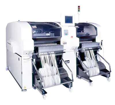
AOI automatic optical inspection instrument
- Categories:Industry News
- Author:Becky Su
- Origin:
- Time of issue:2022-12-09 15:14
- Views:
(Summary description)AOI automatic optical inspection instrument Automated Optical Inspection (AOI, Automated Optical Inspection) I. Definition Using high speed and high precision vision processing technology to automatically detect different kinds of mounting errors and soldering defects on PCB boards. PCB boards can range from fine pitch high density boards to low density large size boards, and can provide in-line inspection solutions to improve production efficiency and solder quality. By using AOI as a defect reduction tool, errors can be found and eliminated early in the assembly process to achieve good process control. Early detection of defects will prevent bad boards from being sent to subsequent assembly stages, and AOI will reduce repair costs by avoiding scrapping unrepairable boards. Second, the main features 1) High-speed inspection system Independent of PCB mounting density (2) Fast and convenient programming system - Graphical interface for -Automatic data inspection with mounting data -Fast editing of inspection data using component database 3)Use of a wealth of special multifunctional inspection algorithms and binary or grayscale (3) Inspection using a wide range of dedicated multifunctional inspection algorithms and binary or grayscale optical imaging processing technology 4) Automatic correction of the detection window according to the instantaneous change of the position of the inspected component Automatic correction to achieve high accuracy detection (5) Detection by marking directly on the PCB with ink or by graphical error representation on the operation display on the operating display with graphic errors to check the detection of electricity
AOI automatic optical inspection instrument
(Summary description)AOI automatic optical inspection instrument
Automated Optical Inspection (AOI, Automated Optical Inspection)
I. Definition
Using high speed and high precision vision processing technology to automatically detect different kinds of mounting errors and soldering defects on PCB boards.
PCB boards can range from fine pitch high density boards to low density large size boards, and can provide in-line inspection solutions to improve production efficiency and solder quality.
By using AOI as a defect reduction tool, errors can be found and eliminated early in the assembly process to achieve good process control. Early detection of defects will prevent bad boards from being sent to subsequent assembly stages, and AOI will reduce repair costs by avoiding scrapping unrepairable boards.
Second, the main features
1) High-speed inspection system
Independent of PCB mounting density
(2) Fast and convenient programming system
- Graphical interface for
-Automatic data inspection with mounting data
-Fast editing of inspection data using component database
3)Use of a wealth of special multifunctional inspection algorithms and binary or grayscale
(3) Inspection using a wide range of dedicated multifunctional inspection algorithms and binary or grayscale optical imaging processing technology
4) Automatic correction of the detection window according to the instantaneous change of the position of the inspected component
Automatic correction to achieve high accuracy detection
(5) Detection by marking directly on the PCB with ink or by graphical error representation on the operation display
on the operating display with graphic errors to check the detection of electricity
- Categories:Industry News
- Author:Becky Su
- Origin:
- Time of issue:2022-12-09 15:14
- Views:
Information
AOI automatic optical inspection instrument
Automated Optical Inspection (AOI, Automated Optical Inspection)
I. Definition
Using high speed and high precision vision processing technology to automatically detect different kinds of mounting errors and soldering defects on PCB boards.
PCB boards can range from fine pitch high density boards to low density large size boards, and can provide in-line inspection solutions to improve production efficiency and solder quality.
By using AOI as a defect reduction tool, errors can be found and eliminated early in the assembly process to achieve good process control. Early detection of defects will prevent bad boards from being sent to subsequent assembly stages, and AOI will reduce repair costs by avoiding scrapping unrepairable boards.
Second, the main features
1) High-speed inspection system
Independent of PCB mounting density
(2) Fast and convenient programming system
- Graphical interface for
-Automatic data inspection with mounting data
-Fast editing of inspection data using component database
3)Use of a wealth of special multifunctional inspection algorithms and binary or grayscale
(3) Inspection using a wide range of dedicated multifunctional inspection algorithms and binary or grayscale optical imaging processing technology
4) Automatic correction of the detection window according to the instantaneous change of the position of the inspected component
Automatic correction to achieve high accuracy detection
(5) Detection by marking directly on the PCB with ink or by graphical error representation on the operation display
on the operating display with graphic errors to check the detection of electricity
Keyword:
Related News


PRODUCTS
CONTACT US
Hotline:(0086)755-27801389
Mobile: (0086)15323874439
Sale No.1: becky@hysmt.cn
Sale No.2: fhysmt@hysmt.cn
Sale No.3: zksale@hysmt.cn
Sale No.4: sale@hysmt.cn
Sale No.5: elsey@hysmt.cn
GIVE ME A MESSAGE
Copyright: ZK Electronic Technology Co., Ltd 粤ICP备11054297号 Powered by www.300.cn