Welcome to ZK Electronic
16 years of industry experience
Good material qualty, high efficiency, fast delivery
搜索
NEWS
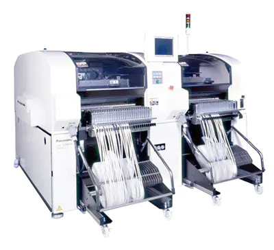
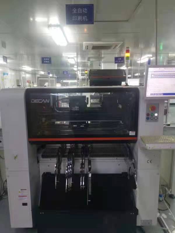
SMT process flow and process description
- Categories:Industry News
- Author:Becky Su
- Origin:
- Time of issue:2023-05-16 16:34
- Views:
(Summary description)SMT process flow and process description 一, chip components single-side mount process 1. Incoming material inspection Description: Check whether the components, pads, solder paste have oxidation, whether the solder composition matches, integrated circuit pins and its coplanarity. 2. Printing solder paste Description:Through solder paste printing machine or SMT solder paste printing table, printing special scraper and SMT leakage board will SMT solder paste leakage printing to the PCB pads. 3. Check the printing effect Description: Check whether the printed circuit board solder paste leakage, adhesion, the amount of solder paste is appropriate, etc. 4.SMD Description:Finish the placement by the placement machine or vacuum suction pen, tweezers, etc. 5. Check SMT placement effect Description: Check whether the posted components are put on the deviation, put on the reverse or leak, and repair, narrow pitch components need to use microscope entity check. 6. Check reflow soldering process setting Description: Check the working conditions of reflow soldering, such as power supply voltage, temperature curve setting, etc. 7. Reflow soldering Description: Reflow soldering by SMT reflow equipment. 8. Check the welding effect and *final inspection Description: Check whether there are welding defects and repair. 二, chip components double-sided placement process 1.Incoming material inspection 2.Screen printing A side solder paste 3. Check the printing effect 4. Mount A-side components, check the effect of SMD 5.Reflow soldering 6.Check the soldering effect 7. Print B-side solder paste 8.Check the printing effect 9. Mount B-side components, check the effect of patching 10.Reflow soldering 11.Repair check 12.* Final inspection Attention matters: 1: A, B side of the distinction is the circuit board in components less and small for A side, components more and large for B side. 2: If both sides have large package components, you need to use a different melting point of the solder paste. That is: A side with high temperature solder paste, B side with low temperature solder paste 3: If there is no different temperature of the solder paste, you need to add a step, that is, after the completion of step 7, you need to A side of the large package components With SMD red glue sticky, and then the B side of the operation. 4: Other steps operation with process (a) 三, research and development in the mixed board placement process 1. incoming material check Description: check whether the components, pads, solder paste have oxidation, whether the solder composition matches, integrated circuit pins and its coplanarity. 2. Drop coating solder paste Description: Use SMT solder paste dispenser, air compressor to drop coating the solder paste in SMT syringe to PCB pads. 3. Check the effect of drip coating Explanation: Check whether the amount of solder paste drip coated is suitable, whether there is leakage of coating or sticking. 4. Placement of components Description:Finished by vacuum suction pen or tweezers, etc. 5. Check the effect of SMD Description: Check whether the pasted components are put on the wrong side, put on the opposite or leak, and repair. 6. Reflow soldering Description: Reflow soldering by HT series desktop small SMT reflow soldering equipment. 7. Check the welding effect Description: Check whether there are welding defects and repair. 8. Solder the plug-in parts Description:Finished by electric soldering iron, solder wire and flux with. 四, double-sided mixed batch production placement process 1.Incoming material check 2. Screen printing A side solder paste 3. Check the printing effect 4. Mount A-side components 5.Check the effect of mounting 6.Reflow soldering 7.Check the soldering effect 8.Printing B-side red glue 9.Check the printing effect 10.Placement of B-side components 11.Check the effect of placement 12.Curing 13.Insert THT components on A side 14.Check the effect of insertion 15.Wave soldering 16.Repair solder joint cleaning test Description: Caution and operation process as described above.
SMT process flow and process description
(Summary description)SMT process flow and process description
一, chip components single-side mount process
1. Incoming material inspection Description: Check whether the components, pads, solder paste have oxidation, whether the solder composition matches, integrated circuit pins and its coplanarity.
2. Printing solder paste Description:Through solder paste printing machine or SMT solder paste printing table, printing special scraper and SMT leakage board will SMT solder paste leakage printing to the PCB pads.
3. Check the printing effect Description: Check whether the printed circuit board solder paste leakage, adhesion, the amount of solder paste is appropriate, etc.
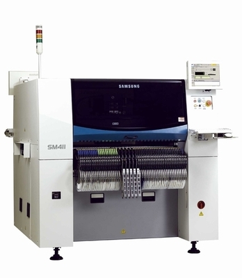
4.SMD Description:Finish the placement by the placement machine or vacuum suction pen, tweezers, etc.
5. Check SMT placement effect Description: Check whether the posted components are put on the deviation, put on the reverse or leak, and repair, narrow pitch components need to use microscope entity check.
6. Check reflow soldering process setting Description: Check the working conditions of reflow soldering, such as power supply voltage, temperature curve setting, etc.
7. Reflow soldering Description: Reflow soldering by SMT reflow equipment.
8. Check the welding effect and *final inspection Description: Check whether there are welding defects and repair.
二, chip components double-sided placement process
1.Incoming material inspection
2.Screen printing A side solder paste
3. Check the printing effect
4. Mount A-side components, check the effect of SMD
5.Reflow soldering
6.Check the soldering effect
7. Print B-side solder paste
8.Check the printing effect
9. Mount B-side components, check the effect of patching
10.Reflow soldering
11.Repair check
12.* Final inspection
Attention matters:
1: A, B side of the distinction is the circuit board in components less and small for A side, components more and large for B side.
2: If both sides have large package components, you need to use a different melting point of the solder paste. That is: A side with high temperature solder paste, B side with low temperature solder paste
3: If there is no different temperature of the solder paste, you need to add a step, that is, after the completion of step 7, you need to A side of the large package components
With SMD red glue sticky, and then the B side of the operation.
4: Other steps operation with process (a)
三, research and development in the mixed board placement process
1. incoming material check Description: check whether the components, pads, solder paste have oxidation, whether the solder composition matches, integrated circuit pins and its coplanarity.
2. Drop coating solder paste Description: Use SMT solder paste dispenser, air compressor to drop coating the solder paste in SMT syringe to PCB pads.
3. Check the effect of drip coating Explanation: Check whether the amount of solder paste drip coated is suitable, whether there is leakage of coating or sticking.
4. Placement of components Description:Finished by vacuum suction pen or tweezers, etc.
5. Check the effect of SMD Description: Check whether the pasted components are put on the wrong side, put on the opposite or leak, and repair.
6. Reflow soldering Description: Reflow soldering by HT series desktop small SMT reflow soldering equipment.
7. Check the welding effect Description: Check whether there are welding defects and repair.
8. Solder the plug-in parts Description:Finished by electric soldering iron, solder wire and flux with.
四, double-sided mixed batch production placement process
1.Incoming material check
2. Screen printing A side solder paste
3. Check the printing effect
4. Mount A-side components
5.Check the effect of mounting
6.Reflow soldering
7.Check the soldering effect
8.Printing B-side red glue
9.Check the printing effect
10.Placement of B-side components
11.Check the effect of placement
12.Curing
13.Insert THT components on A side
14.Check the effect of insertion
15.Wave soldering
16.Repair solder joint cleaning test
Description:
Caution and operation process as described above.
- Categories:Industry News
- Author:Becky Su
- Origin:
- Time of issue:2023-05-16 16:34
- Views:
Information
SMT process flow and process description
一, chip components single-side mount process
1. Incoming material inspection Description: Check whether the components, pads, solder paste have oxidation, whether the solder composition matches, integrated circuit pins and its coplanarity.
2. Printing solder paste Description:Through solder paste printing machine or SMT solder paste printing table, printing special scraper and SMT leakage board will SMT solder paste leakage printing to the PCB pads.
3. Check the printing effect Description: Check whether the printed circuit board solder paste leakage, adhesion, the amount of solder paste is appropriate, etc.
4.SMD Description:Finish the placement by the placement machine or vacuum suction pen, tweezers, etc.
5. Check SMT placement effect Description: Check whether the posted components are put on the deviation, put on the reverse or leak, and repair, narrow pitch components need to use microscope entity check.
6. Check reflow soldering process setting Description: Check the working conditions of reflow soldering, such as power supply voltage, temperature curve setting, etc.
7. Reflow soldering Description: Reflow soldering by SMT reflow equipment.
8. Check the welding effect and *final inspection Description: Check whether there are welding defects and repair.
二, chip components double-sided placement process
1.Incoming material inspection
2.Screen printing A side solder paste
3. Check the printing effect
4. Mount A-side components, check the effect of SMD
5.Reflow soldering
6.Check the soldering effect
7. Print B-side solder paste
8.Check the printing effect
9. Mount B-side components, check the effect of patching
10.Reflow soldering
11.Repair check
12.* Final inspection
Attention matters:
1: A, B side of the distinction is the circuit board in components less and small for A side, components more and large for B side.
2: If both sides have large package components, you need to use a different melting point of the solder paste. That is: A side with high temperature solder paste, B side with low temperature solder paste
3: If there is no different temperature of the solder paste, you need to add a step, that is, after the completion of step 7, you need to A side of the large package components
With SMD red glue sticky, and then the B side of the operation.
4: Other steps operation with process (a)
三, research and development in the mixed board placement process
1. incoming material check Description: check whether the components, pads, solder paste have oxidation, whether the solder composition matches, integrated circuit pins and its coplanarity.
2. Drop coating solder paste Description: Use SMT solder paste dispenser, air compressor to drop coating the solder paste in SMT syringe to PCB pads.
3. Check the effect of drip coating Explanation: Check whether the amount of solder paste drip coated is suitable, whether there is leakage of coating or sticking.
4. Placement of components Description:Finished by vacuum suction pen or tweezers, etc.
5. Check the effect of SMD Description: Check whether the pasted components are put on the wrong side, put on the opposite or leak, and repair.
6. Reflow soldering Description: Reflow soldering by HT series desktop small SMT reflow soldering equipment.
7. Check the welding effect Description: Check whether there are welding defects and repair.
8. Solder the plug-in parts Description:Finished by electric soldering iron, solder wire and flux with.
四, double-sided mixed batch production placement process
1.Incoming material check
2. Screen printing A side solder paste
3. Check the printing effect
4. Mount A-side components
5.Check the effect of mounting
6.Reflow soldering
7.Check the soldering effect
8.Printing B-side red glue
9.Check the printing effect
10.Placement of B-side components
11.Check the effect of placement
12.Curing
13.Insert THT components on A side
14.Check the effect of insertion
15.Wave soldering
16.Repair solder joint cleaning test
Description:
Caution and operation process as described above.
Keyword:
Previous:
Electroplating process and role
Next:
Laminating process
Previous:
Electroplating process and role
Next:
Laminating process
Related News


PRODUCTS
CONTACT US
Hotline:(0086)755-27801389
Mobile: (0086)15323874439
Sale No.1: becky@hysmt.cn
Sale No.2: fhysmt@hysmt.cn
Sale No.3: zksale@hysmt.cn
Sale No.4: sale@hysmt.cn
Sale No.5: elsey@hysmt.cn
GIVE ME A MESSAGE
Copyright: ZK Electronic Technology Co., Ltd 粤ICP备11054297号 Powered by www.300.cn