Welcome to ZK Electronic


Product Series
Feeders/feeder parts, nozzles, filters, lasers, servo motors, drivers, controller boards, solenoid valves, cylinders, ball screws, belts, o-rings, sensors, splice tapes/tools, clean paper rolls; clips, rubber pads, pins, guides, blades, cutters, clamps, squeegees, holders; resistors, capacitors, diodes, inductors, beads, transformers, transistors, fuse, relays, connectors, modules, processors, microcontrollers, logic chips, power chips, memory, amplifiers/linear Devices, ICs etc.

i-PULSE F2-84 feeder board LG4-M1AH1-004
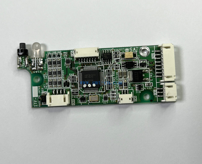
i-PULSE F2-16 feeder board LG4-M1AH1-002
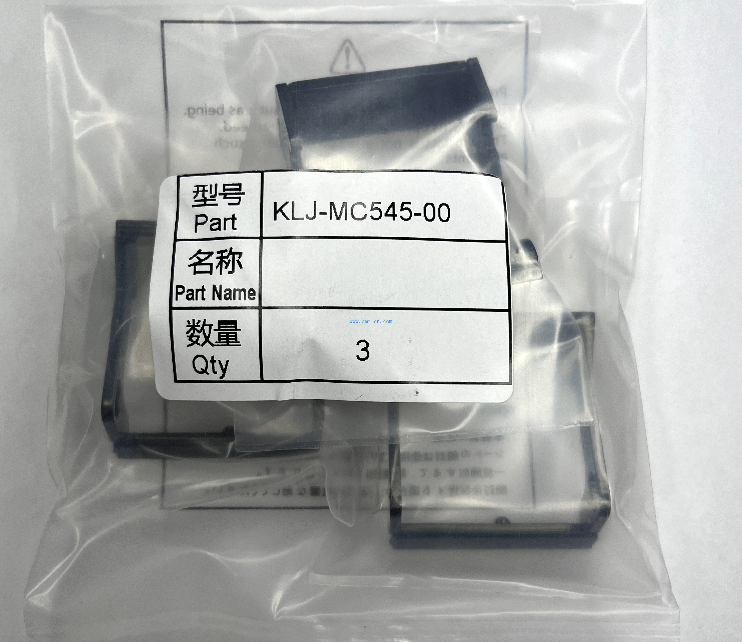
ZS 32MM feeder KLJ-MC545-00 Lever, Tape guide F
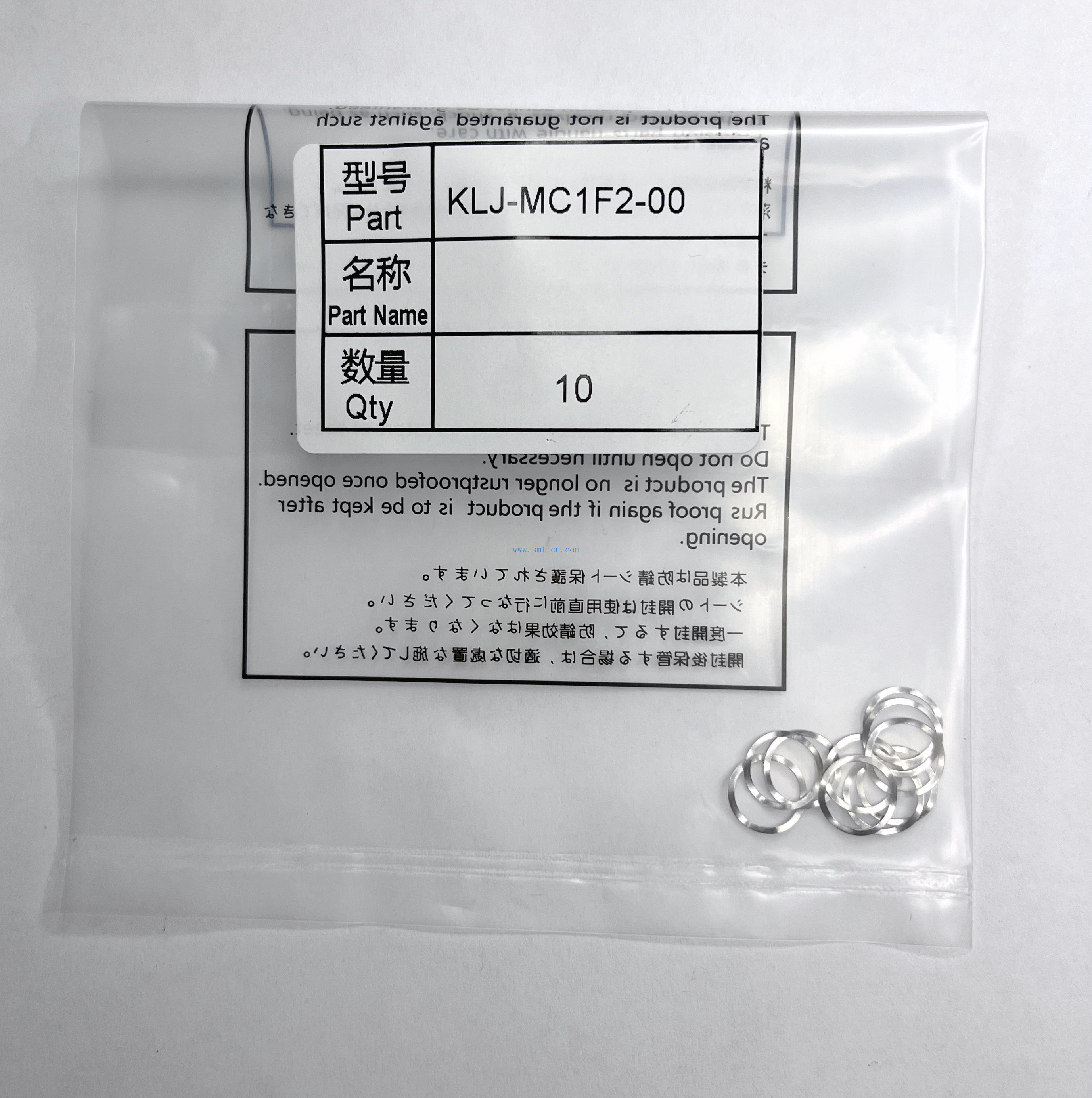
YAMAHA electric feeder Wave Washer KLJ-MC1F2-00

ZS 8mm feeder KLJ-MC163-00 Cover , Tail
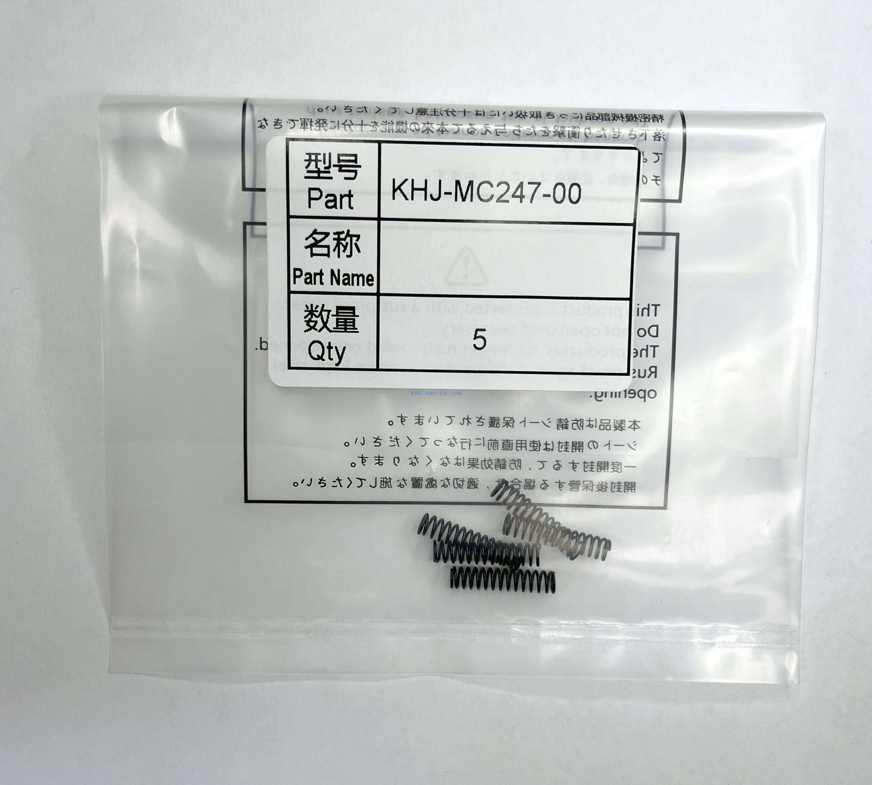
SS 12MM feeder KHJ-MC247-01 Spring , Tape Guide F
ABOUT US
ZK Electronic Technology Co.,Limited
headquarters are located in Shenzhen, China, which is 20 minutes to Shenzhen Airport. ZK was established in 2005, we have two categories:
SMT(Surface-mount technology): highly professional in Surface-Mount Technology area and supports most major brands of electronic assembly equipment with a large selections of original/compatible SMT spare parts, Automatic Insert parts, Printer parts, such as Hanwha(Samsung), Juki, Fuji, Yamaha, Universal, Panasonic(KME), ASM/SIPLACE(SIEMENS), Sony, Sanyo, Hitachi, Assembleon(Phillips), TDK, DEK, GKG, MPM, EKRA,DSP etc. on a quotation basis.
Company Establishment
Engineers Support
Monthly Sales
Success Case
MAIN BUSINESS
1. New/Used SMT lines 2. Chip Mounter/Automatic Insert/Printer parts 3. Electronic components
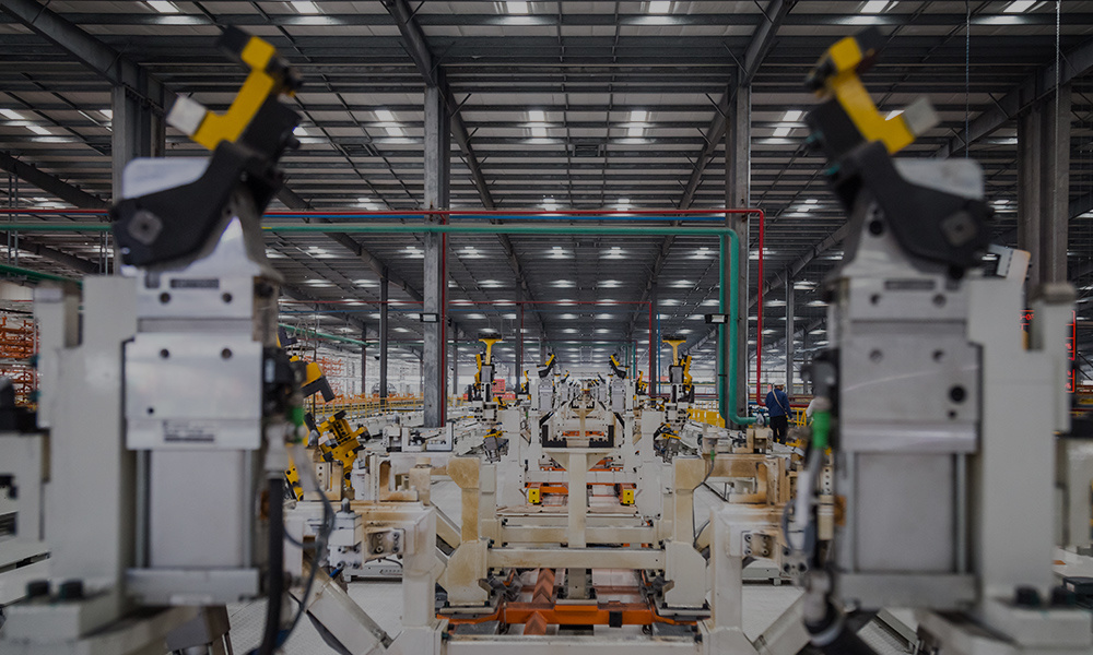
New/Used SMT lines
We Buy, Sell and Trade SMT new & used lines, specifically JUKI, Hanwha(Samsung), Yamaha, Panasonic, FUJI Pick & placement Machines. All equipment leaving our facilities are guaranteed to be fully functional, with no missing parts and in normal working condition.
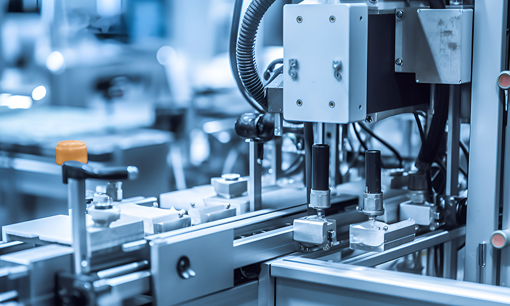
Chip Mounter/Automatic Insert/Printer parts
We have good source and large ready stock for major brands of Chip mounter/Automatic Insert/Printer parts. Such as feeders/feeder parts, nozzles, filters, lasers, servo motors, drivers, controller boards, solenoid valves, ball screws, belts, sensors, splice tapes/tools, clean paper rolls, clips, pins, guides, blades, cutters, clamps, squeegees etc.
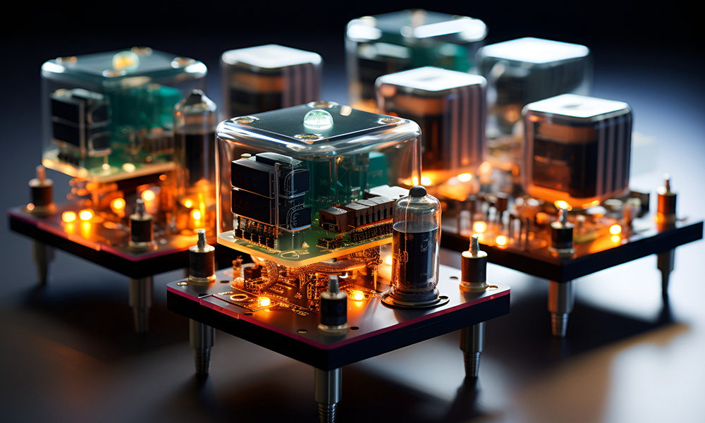
Electronic components
With the mainstream market certifications of CCC, CQC, CE, ROHS, FCC, PSE, UL, etc., ZK products are safe, reliable and quality guaranteed. The electronic components such as resistors, capacitors, diodes, inductors, beads, transformers, transistors, fuse, relays, connectors, modules, processors, microcontrollers, logic chips, power chips, memory, amplifiers/linear Devices, ICs etc.
COOPERATIVE CLIENTS
ZK Electronic Technology Co.,Limited provide Sales, Maintenance & Repair Service of SMT PCB Assembly Equipment, SMT Pick & Place Machines, Printer parts, Automatic Insertion parts, Electronic components for international famous brands.


News
Enterprise Spirit: Credible, Efficient, Dedicated, Pragmatic


Vacuum Head Component YAMAHA Solenoid Valve A010E1-37W for YS12 and YSM10 Models
2026-04-24

Panasonic Placement Machine NPM Mounter head: New and Used Options Available!
2026-04-17
Online Message
The company adheres to the principles of "integrity, efficiency, professionalism, and pragmatism" and is dedicated to providing thoughtful and complete technical and after-sales services as well as first-hand supply for domestic and foreign electronic manufacturers and customers
Contact Us
Contact: Ms. Becky Su
Mobile WeChat WhatsApp: +86-15323874439
Office Tel: 0086-755-27801389
Teams: beckysmt
Factory address :201, 99-2 Dayang Road, XinTian Community, FuHai Street, BaoAn Dist., Shenzhen, Guangdong, China (Mainland)
