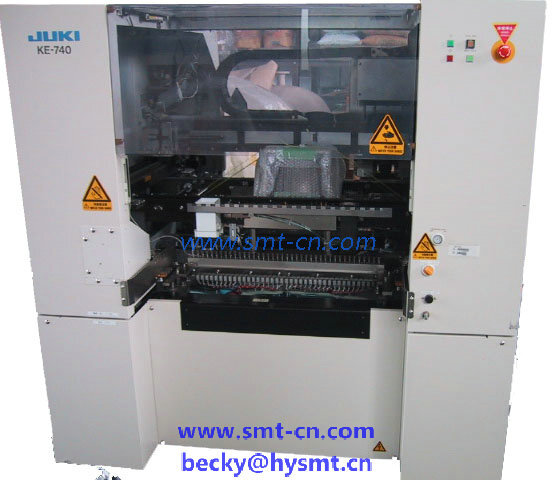
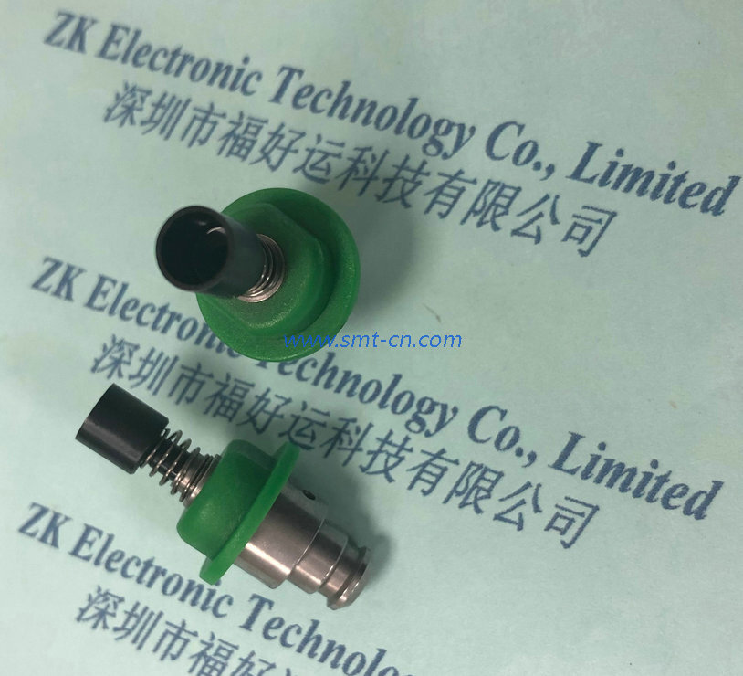
Welcome to ZK Electronic
16 years of industry experience
Good material qualty, high efficiency, fast delivery
搜索
NEWS
How cell phones work
- Categories:Industry News
- Author:Becky Su
- Origin:
- Time of issue:2023-12-15 15:21
- Views:
(Summary description)How cell phones work Cell phones can communicate with each other, mainly by three parts of the coordinated work of the results Respectively for the radio frequency part, the logic part and the power part, to understand the working principle of the cell phone in fact, as long as you understand how these three parts work on it First: radio frequency part Usually the radio frequency part, and by the receiving signal part and send signal part composition. Cell phone in the receiving signal, the first use of the antenna to receive the 935-960MHz RF signal, through the U400, SW363, the receiving signal will be separated from the transmitting signal, so that the send and receive do not interfere with each other. The fourth pin input and fifth pin output from U400 enter the receiving front-end circuit, and the working state of U400 is controlled by the third pin potential, which is in turn controlled by the TXON and RXON signals from the CPU. The RF signal after the antenna switch is first filtered by band-pass filter FL451 and then sent to high-frequency amplifier Q418 for amplification, and the output of Q418 is filtered by FL452 and then sent to Q420 mixer tube for frequency mixing. And the local oscillation signal generated by RXVCO, and FL453 filtered and sent to the base of Q420 for mixing, take the difference, from the collector of Q420 output 153MHz IF signal, filtered by FL420 to get 153MHz pure medium diesel signal, now amplified by the Q421 sent to the 31 feet of the U201, 153MHz IF signal with the The 153MHz IF signal and the 153MHz carrier signal are demodulated in 32D53 to produce RXI and RXQ analog baseband signals, which are sent to U501 at pins 14# and 15# via U201 at 46# and 48#. After A/D conversion in U501, it is sent to the digital signal processor for further processing. 153MHz carrier wave is connected to the 306MHz oscillator circuit composed of peripheral circuits by U201's 41#, 42#, and 43# to form the 306MHz flue-wave signal, which is dichroicly formed into a 153MHz carrier wave. For the transmitting part, the TXIN, TXIP, TXQN, TXQP transmit band signals output from 21#, 22#, 23#, 24# of the 501 enter 61#, 62#, 63#, 64# of the U201. 6#, 7#, 10# of the U201 are connected externally to a 216MHz VCO to generate a 216MHz carrier signal, which is divided by a frequency divider in the U201 to generate a 108MHz carrier signal. The signal is divided by the frequency divider in U201 to generate a 108MHz transmitter IF signal. Four modulation signals in U201 to complete the 108MHz carrier modulation from the fourth pin output to the U300 4 # U300 to complete the launch sampling signal and TXVCO phase gentle frequency, take the difference between the 108MHz signal and the 4 # input TXIF phase identification, resulting in phase identification error voltage from the eighth pin output to control the capacity of the varactor diode CR300 to change the oscillating frequency of TXVCO, from the C pole of Q300 to change the frequency of TXVCO, from the C pole of Q300 to change the frequency of TXVCO, from the C pole of Q300 to change the oscillating frequency of TXVCO. Frequency, from the C pole of Q300 output 890-915MHz transmitter signal by Q301 preamplifier and Q302 drive into the amplifier Q302, amplified signal into the antenna U400 pin 1, and then from the U400 4 # send antenna to transmit out. II: Logic Part In the logic part, the received RXI, RXQ analog baseband signals in the modem U501 internal D / A conversion, decryption and adaptive equalization will be completed after the digital baseband signals from the U501 6 # sent to the CPU 10 # in the CPU for channel decoding, remove the error correction code source as well as take the real control information, the restoration of the voice data flow through the data line and the address line, transmitted to the voice device U801 for decoding. U801 for decoding. The resulting digital voice signal is sent from 78# of U801 to 8# of PCM***U803. Digital voice signals in the PCM **** completed decompression and A/D conversion, and then through the digital volume positioner, the received signal, volume adjustment, and then by the U803 of 4 #, the output analog audio signals to the U900 6 # and 21 #. 6 # input ringing signal, by the internal ringing drive support amplification, from the U900 of 4 #, 5 # output to drive the ringer to send between the audio signal, from 21 # input, through the internal ringing drive support amplification, from the U900 of 4 #, 5 # output to drive the ringer to send between the audio signal, from the U900 of 4 #, 5 # output to drive the ringer to send between the audio signal. Input from 21#, after the internal audio amplifier, from 19#, 20# output amplified voice signal to drive the earpiece sound. When our users are talking, the voice through the earpiece after the conversion of sound and electricity into the power supply integrated circuit U0- 9 #, after the internal audio amplifier, from 10 # output amplified analog audi
How cell phones work
(Summary description)How cell phones work
Cell phones can communicate with each other, mainly by three parts of the coordinated work of the results
Respectively for the radio frequency part, the logic part and the power part, to understand the working principle of the cell phone in fact, as long as you understand how these three parts work on it
First: radio frequency part
Usually the radio frequency part, and by the receiving signal part and send signal part composition. Cell phone in the receiving signal, the first use of the antenna to receive the 935-960MHz RF signal, through the U400, SW363, the receiving signal will be separated from the transmitting signal, so that the send and receive do not interfere with each other. The fourth pin input and fifth pin output from U400 enter the receiving front-end circuit, and the working state of U400 is controlled by the third pin potential, which is in turn controlled by the TXON and RXON signals from the CPU. The RF signal after the antenna switch is first filtered by band-pass filter FL451 and then sent to high-frequency amplifier Q418 for amplification, and the output of Q418 is filtered by FL452 and then sent to Q420 mixer tube for frequency mixing. And the local oscillation signal generated by RXVCO, and FL453 filtered and sent to the base of Q420 for mixing, take the difference, from the collector of Q420 output 153MHz IF signal, filtered by FL420 to get 153MHz pure medium diesel signal, now amplified by the Q421 sent to the 31 feet of the U201, 153MHz IF signal with the The 153MHz IF signal and the 153MHz carrier signal are demodulated in 32D53 to produce RXI and RXQ analog baseband signals, which are sent to U501 at pins 14# and 15# via U201 at 46# and 48#. After A/D conversion in U501, it is sent to the digital signal processor for further processing. 153MHz carrier wave is connected to the 306MHz oscillator circuit composed of peripheral circuits by U201's 41#, 42#, and 43# to form the 306MHz flue-wave signal, which is dichroicly formed into a 153MHz carrier wave. For the transmitting part, the TXIN, TXIP, TXQN, TXQP transmit band signals output from 21#, 22#, 23#, 24# of the 501 enter 61#, 62#, 63#, 64# of the U201. 6#, 7#, 10# of the U201 are connected externally to a 216MHz VCO to generate a 216MHz carrier signal, which is divided by a frequency divider in the U201 to generate a 108MHz carrier signal. The signal is divided by the frequency divider in U201 to generate a 108MHz transmitter IF signal. Four modulation signals in U201 to complete the 108MHz carrier modulation from the fourth pin output to the U300 4 # U300 to complete the launch sampling signal and TXVCO phase gentle frequency, take the difference between the 108MHz signal and the 4 # input TXIF phase identification, resulting in phase identification error voltage from the eighth pin output to control the capacity of the varactor diode CR300 to change the oscillating frequency of TXVCO, from the C pole of Q300 to change the frequency of TXVCO, from the C pole of Q300 to change the frequency of TXVCO, from the C pole of Q300 to change the oscillating frequency of TXVCO. Frequency, from the C pole of Q300 output 890-915MHz transmitter signal by Q301 preamplifier and Q302 drive into the amplifier Q302, amplified signal into the antenna U400 pin 1, and then from the U400 4 # send antenna to transmit out.
II: Logic Part
In the logic part, the received RXI, RXQ analog baseband signals in the modem U501 internal D / A conversion, decryption and adaptive equalization will be completed after the digital baseband signals from the U501 6 # sent to the CPU 10 # in the CPU for channel decoding, remove the error correction code source as well as take the real control information, the restoration of the voice data flow through the data line and the address line, transmitted to the voice device U801 for decoding. U801 for decoding. The resulting digital voice signal is sent from 78# of U801 to 8# of PCM***U803. Digital voice signals in the PCM **** completed decompression and A/D conversion, and then through the digital volume positioner, the received signal, volume adjustment, and then by the U803 of 4 #, the output analog audio signals to the U900 6 # and 21 #. 6 # input ringing signal, by the internal ringing drive support amplification, from the U900 of 4 #, 5 # output to drive the ringer to send between the audio signal, from 21 # input, through the internal ringing drive support amplification, from the U900 of 4 #, 5 # output to drive the ringer to send between the audio signal, from the U900 of 4 #, 5 # output to drive the ringer to send between the audio signal. Input from 21#, after the internal audio amplifier, from 19#, 20# output amplified voice signal to drive the earpiece sound. When our users are talking, the voice through the earpiece after the conversion of sound and electricity into the power supply integrated circuit U0- 9 #, after the internal audio amplifier, from 10 # output amplified analog audi
- Categories:Industry News
- Author:Becky Su
- Origin:
- Time of issue:2023-12-15 15:21
- Views:
Information
How cell phones work
Cell phones can communicate with each other, mainly by three parts of the coordinated work of the results
Respectively for the radio frequency part, the logic part and the power part, to understand the working principle of the cell phone in fact, as long as you understand how these three parts work on it
First: radio frequency part
Usually the radio frequency part, and by the receiving signal part and send signal part composition. Cell phone in the receiving signal, the first use of the antenna to receive the 935-960MHz RF signal, through the U400, SW363, the receiving signal will be separated from the transmitting signal, so that the send and receive do not interfere with each other. The fourth pin input and fifth pin output from U400 enter the receiving front-end circuit, and the working state of U400 is controlled by the third pin potential, which is in turn controlled by the TXON and RXON signals from the CPU. The RF signal after the antenna switch is first filtered by band-pass filter FL451 and then sent to high-frequency amplifier Q418 for amplification, and the output of Q418 is filtered by FL452 and then sent to Q420 mixer tube for frequency mixing. And the local oscillation signal generated by RXVCO, and FL453 filtered and sent to the base of Q420 for mixing, take the difference, from the collector of Q420 output 153MHz IF signal, filtered by FL420 to get 153MHz pure medium diesel signal, now amplified by the Q421 sent to the 31 feet of the U201, 153MHz IF signal with the The 153MHz IF signal and the 153MHz carrier signal are demodulated in 32D53 to produce RXI and RXQ analog baseband signals, which are sent to U501 at pins 14# and 15# via U201 at 46# and 48#. After A/D conversion in U501, it is sent to the digital signal processor for further processing. 153MHz carrier wave is connected to the 306MHz oscillator circuit composed of peripheral circuits by U201's 41#, 42#, and 43# to form the 306MHz flue-wave signal, which is dichroicly formed into a 153MHz carrier wave. For the transmitting part, the TXIN, TXIP, TXQN, TXQP transmit band signals output from 21#, 22#, 23#, 24# of the 501 enter 61#, 62#, 63#, 64# of the U201. 6#, 7#, 10# of the U201 are connected externally to a 216MHz VCO to generate a 216MHz carrier signal, which is divided by a frequency divider in the U201 to generate a 108MHz carrier signal. The signal is divided by the frequency divider in U201 to generate a 108MHz transmitter IF signal. Four modulation signals in U201 to complete the 108MHz carrier modulation from the fourth pin output to the U300 4 # U300 to complete the launch sampling signal and TXVCO phase gentle frequency, take the difference between the 108MHz signal and the 4 # input TXIF phase identification, resulting in phase identification error voltage from the eighth pin output to control the capacity of the varactor diode CR300 to change the oscillating frequency of TXVCO, from the C pole of Q300 to change the frequency of TXVCO, from the C pole of Q300 to change the frequency of TXVCO, from the C pole of Q300 to change the oscillating frequency of TXVCO. Frequency, from the C pole of Q300 output 890-915MHz transmitter signal by Q301 preamplifier and Q302 drive into the amplifier Q302, amplified signal into the antenna U400 pin 1, and then from the U400 4 # send antenna to transmit out.
II: Logic Part
In the logic part, the received RXI, RXQ analog baseband signals in the modem U501 internal D / A conversion, decryption and adaptive equalization will be completed after the digital baseband signals from the U501 6 # sent to the CPU 10 # in the CPU for channel decoding, remove the error correction code source as well as take the real control information, the restoration of the voice data flow through the data line and the address line, transmitted to the voice device U801 for decoding. U801 for decoding. The resulting digital voice signal is sent from 78# of U801 to 8# of PCM***U803. Digital voice signals in the PCM **** completed decompression and A/D conversion, and then through the digital volume positioner, the received signal, volume adjustment, and then by the U803 of 4 #, the output analog audio signals to the U900 6 # and 21 #. 6 # input ringing signal, by the internal ringing drive support amplification, from the U900 of 4 #, 5 # output to drive the ringer to send between the audio signal, from 21 # input, through the internal ringing drive support amplification, from the U900 of 4 #, 5 # output to drive the ringer to send between the audio signal, from the U900 of 4 #, 5 # output to drive the ringer to send between the audio signal. Input from 21#, after the internal audio amplifier, from 19#, 20# output amplified voice signal to drive the earpiece sound. When our users are talking, the voice through the earpiece after the conversion of sound and electricity into the power supply integrated circuit U0- 9 #, after the internal audio amplifier, from 10 # output amplified analog audio signal. The signal is sent to the PCM coder ****U803 18 # in the U803 internal PCM coding is completed. From 13 # output PCM signal to the voice encoder 801 of 89 #, in the U801 into the voice data line and address line will be the voice data stream pounds to the central processor U701, the voice data stream in the U701 after the completion of the channel coding, through the U701 of 11 # sent to the modulation demodulator U501 of the 4 #, the signal in the U501 for D / A conversion, encryption and other processing, after the After D/A conversion, encryption and other processing in U501, the four modulated signals TXIP, TXIN, TXQP, TXQN are sent to the transceiver IF circuit U201 to produce ** RF IF ITX, IF signals.
Three: power supply part
As for the power supply part, once we put the battery on the cell phone, the electronic Q999 is turned on; at the same time, the 48# of 32D54 is connected to the positive pole of the power supply, at this time, if we press the power-on button again, the 24# of U900 becomes low, and the regulated output of U900 outputs four voltages, respectively, R275V, L2.75V, R4.75V, and L5.0V. 30# produces a reset signal and the 27# produces a power-on application signal. No. 27# generates the power-on application signal. The 13MHz clock oscillator is composed of 32D53, 13MHz crystal and voltage-variable diode, which generates a 13MHz clock, which is shaped and amplified in 32D53, and then outputs from 59# to send the buffer interface circuit U703 to 17#, and then sends the power-on sustaining signal from 37# to CPU 50# to U900 to maintain the power-on normal 29#. In addition, the collector voltage of Q202 and Q203 are both 2.75V, supplying power to the internal receiving or transmitting circuits of 32D53. L5.0V sent from U900's #3 sends power to the negative voltage generating circuit. Version, SIM card and PCM programmer*** U803 is also L5.0V power supply. 28# of U900 sends out R2.75V to supply power to all logic modules. 28# of U900 sends out 2.75V to supply power to RF section. 41# of U900 sends out R4.75V to supply power to transceiver and IF circuits 32D53 generation. 37# of U900 outputs the VXW conversion voltage supplies power to the emitters of Q202 and Q203.
Due to the different models of cell phones and manufacturers, the above working principle may not apply to some cell phones, but the general workflow should be the same.
Keyword:
Related News


PRODUCTS
CONTACT US
Hotline:(0086)755-27801389
Mobile: (0086)15323874439
Sale No.1: becky@hysmt.cn
Sale No.2: fhysmt@hysmt.cn
Sale No.3: zksale@hysmt.cn
Sale No.4: sale@hysmt.cn
Sale No.5: elsey@hysmt.cn
GIVE ME A MESSAGE
Copyright: ZK Electronic Technology Co., Ltd 粤ICP备11054297号 Powered by www.300.cn